


Why the US is Going All Out Against Huawei's Ascend Chips: A "Light-Speed" Counteroffensive and Containment in the Battle for AI Supremacy
From the "Street Fights" of Chip Interconnects to the "Fiber Optic Superhighway": Unveiling How Huawei's CloudMatrix Supernode is Rattling the US

The US Department of Commerce recently unleashed another heavy-handed blow, targeting Huawei's Ascend AI chips with unprecedentedly severe restrictions. Many might wonder: why such an intense reaction to a single Huawei chip line? The answer lies not just in the chip's performance, but in an "interconnect technology" revolution poised to reshape the global AI landscape. This article uses vivid analogies and clear analysis to explore how Huawei is forging a new path, attempting to use "light" to string together AI computing clusters that surpass traditional methods, and why this has struck America's most sensitive nerve. This isn't just a tech war; it's a mirror reflecting future industrial paradigms and international competition, offering profound food for thought for every reader in Taiwan navigating the tech wave.
The hottest topic circling the tech world recently is undoubtedly the incendiary new regulations from the U.S. Department of Commerce: a global ban on Huawei's Ascend chips, strict prevention of chip transshipments to China, and a prohibition on U.S. chips powering Chinese large language models. Each move is ruthless, seemingly designed to extinguish any spark Huawei might ignite in the AI field. A big question looms in everyone's mind: What is the United States truly afraid of? Do Huawei's Ascend chips really possess such power?
The answer, perhaps, lies in a term many are still unfamiliar with: Huawei's CloudMatrix 384 Supernode. This innovation might be Huawei's secret weapon to bypass U.S. chip blockades and pull off a “corner‑overtaking” maneuver in AI computing power.
THE “GANG FIGHT” ERA IN AI: COMPUTING POWER ISN’T JUST “1+1”
Imagine a scenario: you have two incredibly intelligent workers (chips) simultaneously tackling a complex task—like training a large AI model. Intuitively, two people should be faster than one, right? But what if these two workers communicate as if playing charades, fumbling task allocation and progress reports? One might finish the job while the other is still clueless. In that case, two—or even ten—people may be less efficient than a single, well‑coordinated operative.
This is the art of stacking AI chips. Today’s large language models, with parameters numbering in the hundreds of billions or even trillions, are like super‑thick encyclopedias—one chip card simply can’t hold it all. Hundreds or even thousands of cards must join hands and hearts, like a highly coordinated army, to shoulder the training and inference load.
It’s like the shift from one‑on‑one duels to gang fights: teamwork rules. Can chips be effectively stacked? How much potential can each chip unleash inside a massive cluster? The key lies in their communication speed and methods.
THE “HIGHWAY SYSTEM” INSIDE YOUR COMPUTER: FROM REGULAR ROADS TO SUPERHIGHWAYS

Most hardware in a computer connects through PCIe, the ordinary road network criss‑crossing the motherboard. For everyday tasks, it’s fine. But when several GPUs—the main workhorses for AI—need to run flat‑out, processing oceans of data and constantly exchanging notes, PCIe jams up fast.
Worse, PCIe uses a master‑slave architecture. The CPU is the boss; everything else is an employee. If employees want to talk, they must route requests through the boss. That round‑trip drags efficiency.
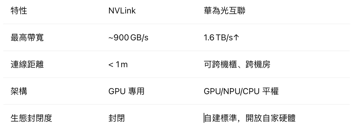
Nvidia felt this pain early. Back in 2014, it rolled out NVLink, a VIP lane connecting GPUs directly. Building on that, NV Switch lets many GPUs chat as peers at a round table, no CPU permission slips required. This dedicated lane is ten—sometimes twenty—times faster than PCIe.
That’s why even the neutered H20 chips sold to China — less than one‑third the performance of U.S.‑market H100s — are still hot commodities: Chinese firms can rely on NVLink to squeeze respectable returns out of big GPU stacks and keep their models alive.
NVLink ACHILLES’ HEEL: DISTANCE IS A MAJOR CONSTRAINT
NVLink’s super‑lane has two Achilles’ heels.
Purebred only. NVLink is GPU‑to‑GPU within Nvidia’s own family. To talk with CPUs or anything else, traffic detours back to pedestrian PCIe, slowing everything down.
Social‑distance limits. NVLink’s reach is short. On the same board, fine; between boards you need copper cables, and signals degrade beyond about a meter—like Bluetooth headphones cutting out when you stray too far from your phone.
To stack big GPU armies, Nvidia squeezes them into the tightest space possible. Its flagship rig stuffs 72 top‑tier GB200 chips into a custom cabinet, tied together by NVLink—a supernode. That’s the best Nvidia can do today. Need more? Linking two such cabinets forces you onto InfiniBand or high‑speed Ethernet — an instant 10× speed drop.
HUAWEI’S COUNTERSTRIKE: A “BRIGHT” PATH FORGED FROM DESPERATION
The plot twist came in 2019, when the U.S. ejected Huawei from the PCIe standards group. Losing the ordinary roads looked fatal.
Backed into a corner, Huawei said, “Fine — new road.” From scratch, it built a fresh communication fabric free of legacy baggage, tapping its greatest strength: optical‑communications know‑how.
Picture every chip sporting a tiny optical module. Electrical signals convert instantly to light, racing along hair‑thin fiber. This fiber‑optic superhighway offers:
• Massive bandwidth. Parallel lanes push aggregate bandwidth into the hundreds of gigabytes per second — faster than NVLink.
• Equal footing. GPU, CPU, NPU — everyone’s a peer, no single boss.
• Distance agnostic. Whether inside one chassis, across racks, or across the entire data center, speed holds steady.
Enter CloudMatrix 384, a supernode of 384 Ascend chips bonded by light. SEMI Analysis estimates its total throughput at roughly 2.2× that of NVIDIA’s 72‑card GB200 supernode — proof that smart system design can let “quantity beat quality.”
The 384‑card scale also unlocks wins for models like Deepseek’s Mixture‑of‑Experts setup with 256 experts: each expert can claim a dedicated card, eliminating contention and latency.
A ban‑induced workaround became Huawei’s sharpest sword.
WHY DOESN’T NVIDIA USE LIGHT?
Nvidia flirted with optical links for 256 H100s in 2022 but shelved the idea. Officially: optical modules are pricey and power‑hungry. Beneath the surface: fiber systems are fragile. Loose connectors, bent fiber, a speck of dust — any minor glitch drops the link. Copper looks like a battle‑hardened mule by comparison.
Large‑scale optical would force NVIDIA to buy delicate parts it doesn’t fully control and shoulder endless maintenance headaches — so it doubled down on copper.
HUAWEI WAS ORIGINALLY A TELECOMMUNICATIONS EQUIPMENT MANUFACTURER
Huawei, by contrast, grew up in telecom. It was building network switches in the 1990s and hit world‑class optical‑comm levels by 2000. String together all the fiber Huawei has laid and it might wrap Earth dozens of times.
A few examples of its chops:
• AI‑powered fault prediction. Sub‑healthy optical modules betray themselves via tiny drifts in power, current, voltage, temperature. Huawei Cloud’s algorithms flag a dying module and swap it before failure.
• Damage‑resistant rerouting. If one fiber lane collapses, Huawei Cloud throttles other lanes and keeps traffic — and model training — flowing. The company says this slashes failure rates and lets training run 40+ days nonstop.
• Self‑healing diagnostics. Dynamic stress tests pinpoint failing nodes, match them to a library of tens of thousands of fault modes, and trigger minute‑level automated recovery.
What looks like a hot potato to NVIDIA is home turf for Huawei. And because Huawei sells Ascend AI Cloud services, customers never touch the plumbing — spin up as few as five chips and you’re off.
As for optical power draw: China is the world’s largest energy producer, especially in renewables. Burning a bit more juice beats living under the U.S. thumb.
DIFFERENT PATHS, SIMILAR DESTINATIONS: NATIONAL STRENGTHS SHAPE TECHNOLOGICAL ROUTES
Nvidia excels at squeezing extreme performance from each chip and packing those elite soldiers into a tight unit — single‑point brilliance. Huawei orchestrates vast numbers of solid soldiers through superior communications — system‑level supremacy.
The divergence mirrors national ecosystems:
• Nvidia’s single‑chip muscle was forged by America’s 3D‑gaming and pro‑graphics scenes, which prize peak per‑chip performance.
• Huawei’s optical edge was nurtured by China’s massive fiber‑to‑the‑home rollout — now 90 percent penetration versus roughly 30 percent in the U.S. — giving it unmatched scale and maintenance experience.
The U.S. assault on Ascend targets not just a chip but a rival technology path — system‑level optical interconnects that threaten America’s AI infrastructure dominance.
Sanctions may sting Huawei short‑term but will likely accelerate China’s homegrown breakthroughs. The lightspeed offensive‑defensive game around AI compute is only starting.
For Taiwan, perched at a pivotal spot in the global tech chain, grasping the logic behind this clash and plotting its own course is critical. Where will the tech map go next? The clues lie in these technical details and strategic showdowns.
美國商務部近期再出重拳,劍指華為昇騰AI晶片,禁令之嚴厲前所未見。許多朋友或許納悶,為何華為一款晶片,竟能引發美國如此強烈的反應?這背後,不僅僅是晶片本身的性能,更關乎一場正在重塑全球AI版圖的「互聯技術」革命。本文將用生動的比喻和深入淺出的分析,帶您一探究竟:華為如何另闢蹊徑,試圖用「光」串聯起超越傳統的AI算力集群,以及這為何觸動了美國最敏感的神經。這不只是一場科技戰,更是一面映照未來產業格局與國際競合的鏡子,值得身處科技浪潮中的每一位台灣讀者深思。
最近,科技圈最熱的話題莫過於美國商務部那幾條火藥味十足的新規:全球禁用華為昇騰晶片、嚴防晶片轉運中國、禁止美國晶片驅動中國大模型。招招狠辣,彷彿要將華為在AI領域的任何一絲火花都徹底掐滅。大家心裡可能都有個大問號:美國到底在怕什麼?華為的昇騰晶片,真有這麼大的「威力」嗎?
答案,或許就藏在一個許多人還很陌生的名詞裡 —— 華為CloudMatrix 384超節點。這玩意兒,可能就是華為找到的,繞開美國晶片封鎖,實現AI算力「彎道超車」的秘密武器。

AI界的「群毆」時代:算力不是簡單的「1+1」
想像一個場景:您有兩個超級聰明的工人(晶片)同時做一件複雜的工作(例如訓練一個大型AI模型)。直覺上,兩個人肯定比一個人快吧?但如果這兩位工人溝通起來像打啞謎,分配任務、匯報進度都慢吞吞,那很可能其中一位早就把活幹完了,另一位還在「狀況外」。這時候,兩個人,甚至十個人,效率都未必比得上一個配合默契的單兵。
這就是AI晶片「堆疊」的學問。現在的AI大模型,動輒幾千億甚至上萬億個參數,像一本超級厚的百科全書,一張小小的晶片卡肯定「裝不下」。這就需要成百上千張晶片卡「手牽手、心連心」,像一個高度協同的軍團,才能扛起訓練和運行的重任。
這就好比以前打架是「一對一單挑」,我可能打不過你;但現在是「群毆」的時代,講究的是團隊協作。晶片能不能有效「堆」起來?每一塊晶片在龐大的集群裡,到底能發揮出多少潛力?關鍵,就在於它們之間的「溝通速度」和「溝通方式」。
電腦裡的「公路系統」:從普通公路到超級專線
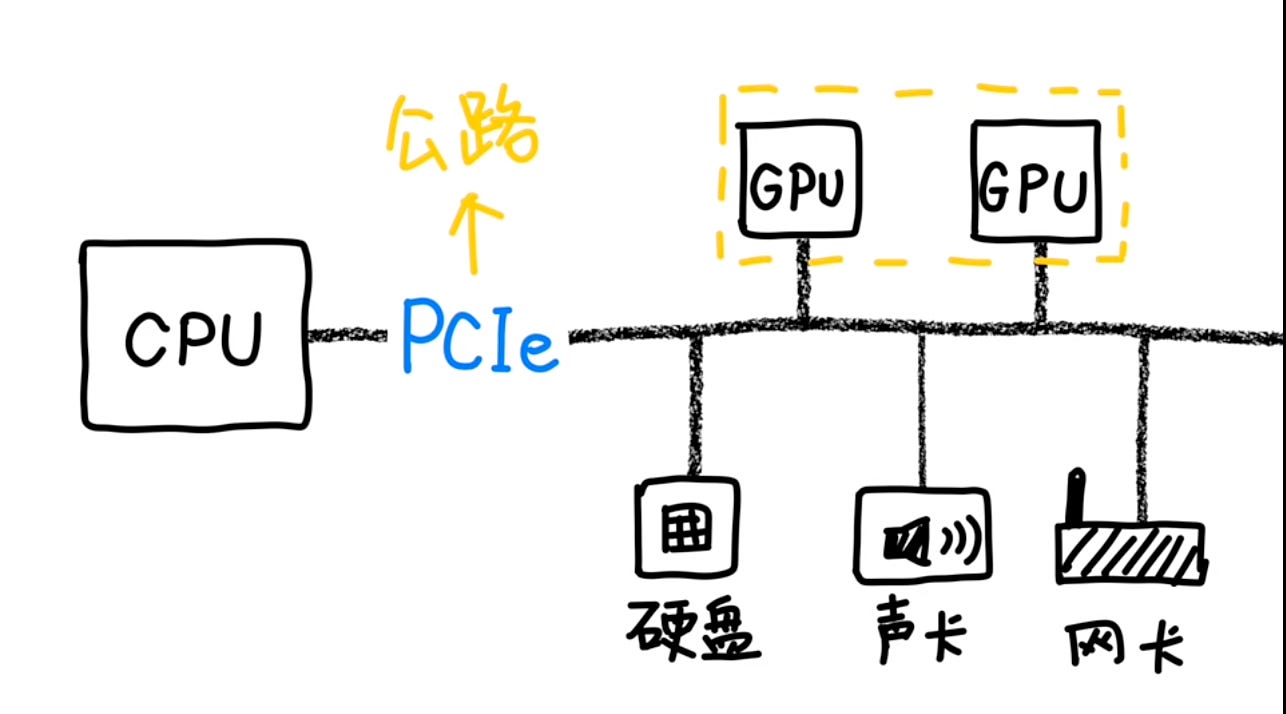
我們電腦裡的各種硬體,大多時候靠一個叫做「PCIe」的通道互相連接。您可以把它想像成電腦內部四通八達的「普通公路網」。日常使用,這路網綽綽有餘。但當好幾個GPU(圖形處理器,AI運算的主力)要火力全開,處理海量數據,頻繁交換「意見」時,PCIe這條「普通公路」就開始大塞車了。
更麻煩的是,PCIe是一種「主從架構」。CPU(中央處理器)像是「老闆」,其他設備都是「員工」。員工之間要溝通,還得先請示老闆,由老闆統一調度。這一來一回,效率自然大打折扣。
AI晶片巨頭輝達(Nvidia)深知此痛點。早在2014年,他們就搗鼓出了一條GPU之間的「VIP專線」—— NVLink。並且以此為基礎,打造了NVSwitch,讓更多的GPU可以像開圓桌會議一樣,直接對等互聯,不用再事事請示CPU老闆。這條「專線」的速度,比PCIe快上十幾甚至二十多倍!
這也是為什麼,即使是賣給中國市場的「閹割版」晶片H20(性能不到美企能買到的H100的三分之一),中國企業依舊搶破頭。因為它們可以用NVLink高速互聯,讓「堆卡」的實際算力收益更高,勉強維持AI模型的運轉。
NVLink的距離是最大硬傷
不過,NVLink這條「超級專線」也有兩個小小的「阿基里斯腱」:
「血統純正」要求高:只有輝達自家的GPU之間才能走NVLink。GPU要跟其他零件(比如CPU)溝通,還是得繞回PCIe那條「普通公路」,整體速度依然會被拖累。
「社交距離」有限制:NVLink的傳輸距離是個大問題。如果GPU在同一塊電路板上,走的是板上的「微型電線」;如果是不同電路板,通常需要用銅纜連接。在高速傳輸下,這些銅纜超過一米,信號就會像手機藍牙耳機離太遠一樣,開始卡頓、斷連。
所以,輝達要堆疊大量GPU,只能想盡辦法把它們「壓縮」到一個極小的空間裡。例如,他們最頂尖的方案,就是把72個最強的GB200晶片「塞」進一個特製的機櫃裡,用NVLink緊密相連,形成一個「超節點」。這已經是輝達目前能交出的最佳答卷了。想堆更多?比如兩個這樣的超節點要互聯,對不起,只能走長距離的傳輸網路(如InfiniBand,高速乙太網),速度立刻比NVLink慢上10倍,溝通效率大打折扣。
華為的「絕地反擊」:被逼出來的「光」明大道
故事的轉折點發生在2019年。美國一紙禁令,華為被踢出了由美國企業主導的PCIe標準組織的「朋友圈」。這意味著,華為連電腦裡的「普通公路」都快沒得用了,簡直是釜底抽薪。
俗話說,「關上一扇門,必然會打開一扇窗」。被逼到牆角的華為,索性心一橫:既然舊路不通,我就自己開闢一條新路!他們決定從頭打造一套全新的通信方案,連接各種晶片和設備。
正是因為這套方案「全新」,沒有歷史包袱,反而讓華為得以放開手腳,將自身最大的優勢發揮到極致。這個優勢是什麼?光通信技術。
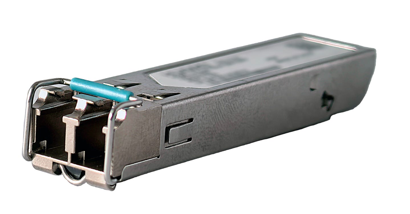
想像一下,華為給每個晶片都裝上了一個小巧的光模塊,把晶片產生的電信號,即時翻譯成「光信號」,然後用比頭髮絲還細的光纖來傳輸。
這條「光纖大道」有幾個驚人的優勢:
超級寬頻:通過多路並行,帶寬可以累加到每秒幾百GB,比輝達的NVLink還要快!
眾生平等:無論你是GPU、CPU還是NPU(神經網路處理器),大家都能用這套系統,而且在架構上完全對等,沒有誰是絕對的「老闆」。
無視距離:這點最為關鍵!光纖傳輸幾乎不受距離限制。無論是在一個機箱內、不同機櫃間,甚至跨越整個數據中心,都能保持高速暢通。
於是,一個由384個昇騰晶片通過光纖高速互聯組成的CloudMatrix 384超節點,橫空出世。這就是華為在AI算力戰場上交出的答卷。
核心概念:把電訊號直接轉為光訊號,再以光纖傳輸,距離不再是瓶頸。
根據專業分析機構SEMI analysis的報告,華為這個「巨無霸」超節點的整體計算能力,竟然是輝達超節點的兩倍多!(單櫃 384 張昇騰 910C,整體吞吐約為 NVIDIA 72 張 GB200 超節點的 2.2 倍。)這種「以多打少」、「用系統規模彌補單卡差距」的策略,讓華為(以及中國的AI產業)在特定場景下,突然擁有了超越輝達的AI系統級能力。
而且,384個晶片的龐大規模還帶來了意想不到的好處。例如,現在很紅的MoE(專家混合)模型,像是Deepseek,它內部就由256個「專家模型」構成。如果跑在輝達那72張卡的超節點上,要嘛好幾個「專家」擠在一張卡裡互相搶資源,要嘛分散在好幾個超節點裡,忍受跨節點的通信延遲。但如果跑在華為這384張卡組成的超節點裡,簡直是量身訂做——每個「專家」都能分到一張卡,獨立思考,效率自然大大提升。
誰能想到,當年被美國制裁逼出來的自研傳輸方案,反而成了華為在AI時代最有力的回擊武器?
輝達為何不用「光」?
一定有朋友會問:「既然光通信這麼厲害,為啥輝達不用它來堆更多晶片呢?」輝達其實在2022年就曾計劃用光通信連接256個H100晶片,但後來放棄了。
明面上的原因是:光模塊太貴,而且功耗太大。但更深層次的原因是,光通信系統比傳統銅纜更容易出故障。插孔沒插緊、光纖彎折得狠了點、插頭沾了點灰塵……各種看似微不足道的小問題,都可能導致通信中斷。相比之下,銅纜簡直像頭老黃牛,皮實耐造,脾氣又好。
如果輝達要大規模採用光通信,就得向其他公司採購光模塊等關鍵組件。這些東西本來就嬌貴易損,輝達還無法自己掌控質量,後期的維護簡直是個無底洞。所以,輝達最終選擇了「退而求其次」,繼續深耕銅纜互聯技術。
華為本來就是一家通訊設備製造廠
然而,華為本就是做通信起家的巨頭。上世紀90年代就開始研發網路交換機,2000年前後,華為的光通信技術就已經達到了國際領先水平。如果把華為過去鋪設和應用過的光通信總長度連起來,估計都能繞地球好幾十圈了!這背後積累了多少經驗和技術,可想而知。
我隨便舉幾個例子,您就能感受到華為的「功力」:
AI神算子,預判故障:在光通信發生故障前,光模塊往往會處於一種「亞健康」狀態。華為雲可以通過AI演算法,根據光模塊的收發功率、電流、電壓、溫度等細微變化,提前判斷出哪個光模塊快「不行了」,在它徹底「罷工」前就主動更換。
「斷路求生」的抗損技術:某個光通信通道突發故障,就好比高速公路上一個車道突然塌方,通常整條路都可能堵死癱瘓。但華為雲可以實現「臨時封閉故障車道,協調其他車道降速限行」,讓整體交通(模型訓練)依然保持通暢,不至於中斷。根據華為官方的說法,通過這項技術,可以大幅降低光模塊的失效率,讓模型訓練穩定運行40天以上不中斷!
「神醫快診」的自愈系統:一旦發生故障,系統可以通過動態的壓力測試技術,快速定位是哪個節點「拖後腿」。然後,再從內置的上萬種故障模式庫中,精準識別出到底是什麼問題,並觸發相應的自愈策略,做到分鐘級的自動恢復。
這些看似神奇的「獨門絕技」,都不是一朝一夕之功,而是靠著無數工程師在無數次的實踐和「踩坑」中,一點一滴積累出來的。
所以,光通信對輝達可能是「燙手山芋」,但對華為來說,簡直是「看家本領」。更何況,華為是以「昇騰AI雲服務」的方式向客戶提供算力。客戶根本不用操心光通信的維護問題,即開即用,想用多少算多少,哪怕只用5個、10個晶片也可以。
至於光模塊功耗大的問題,中國是全球最大的能源生產國,也是最大的清潔能源生產國。為了發展AI這種戰略級技術,稍微多用點電,總比時刻看美國臉色要強得多。
兩條路線的殊途同歸:國家稟賦決定科技路徑
回過頭來看,您會發現一個有趣的現象:
輝達,強在單張晶片的極致性能,然後想辦法把這些「精兵強將」盡可能壓縮在一個小空間裡,靠的是「單點突破,局部最優」。
華為,則另闢蹊徑,用超強的通信能力把數量更多的「普通士兵」高效組織起來,形成規模龐大的「集團軍」,靠的是「系統整合,整體超越」。
這兩條不同的技術路線,其實與中美兩國各自的產業土壤和國家稟賦息息相關:
輝達超強的單卡能力,最早是被美國高度發達的3D遊戲和專業圖形計算產業,「內卷」出來的。那是對單點渲染能力、圖形處理速度的極致追求。
華為超強的通信能力,則很大程度上是被中國超高的光纖到戶普及率,「倒逼」和「滋養」出來的。中國從1991年就開始大力發展光纖通信,如今光纖入戶普及率高達90%,而美國僅有30%左右。這種大規模、高密度的光網路建設和運維經驗,是華為在光通信領域獨步全球的基石。
歷史的發展軌跡,往往在不經意間決定了我們比競爭對手更擅長什麼。美國死掐華為昇騰晶片,正是因為華為CloudMatrix 384超節點所代表的這種「系統級光互聯」能力,實實在在地撼動了美國在AI算力基礎設施領域的霸權根基。這不再是單個晶片性能的較量,而是一種全新技術路徑的挑戰。
美國的制裁,或許短期內會給華為帶來巨大困難,但從長遠看,也可能倒逼中國加速在核心技術領域的自主研發。這場圍繞AI算力的「光速」攻防戰,才剛剛開始。對於身處全球科技產業鏈關鍵位置的台灣而言,看清這背後的深層邏輯,思考自身在變局中的定位與策略,無疑具有極其重要的現實意義。未來,科技的版圖將如何演變?或許,答案就藏在這些看似遙遠的技術細節與國家戰略的交鋒之中。